
Printed circuit boards (PCBs) are integral components of nearly all modern electronic devices. Used in everything from smartphones to CT scanners, these sophisticated modules are manufactured in a range of custom sizes and configurations to meet various device-specific requirements. With the recent trend toward smaller, faster, and more powerful electronic devices, PCB manufacturing has become increasingly important in a number of fast-paced, demanding industries.
What is a Printed Circuit Board?
PCBs are thin, flat structures inscribed with conductive pathways and pads that allow capacitors, resistors, and other electronic components to be physically supported and electrically connected. Components can be soldered, or mechanically fastened, to one or both sides of the board’s metal pads, forming either a single layer of circuitry or multiple layers stacked together. Linked to the board’s circuitry, the metal pads facilitate interconnections among the various electrical components. While most PCBs are rigid, some are manufactured with flexible or semi-flexible substrates that allow the circuitry to bend and flex into various shapes.
Printed Circuit Board Materials
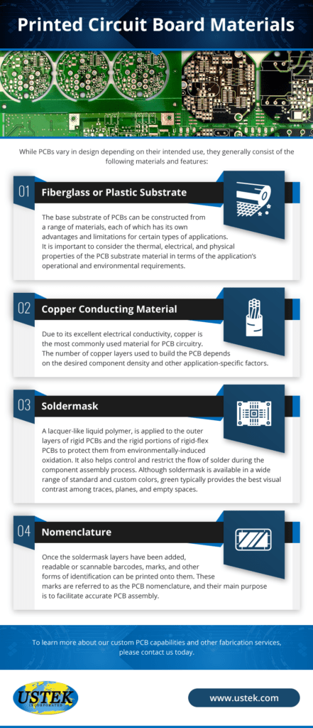
While PCBs vary in design depending on their intended use, they generally consist of the following materials and features:
- Fiberglass or plastic substrate. The base substrate of PCBs can be constructed from a range of materials, each of which has its own advantages and limitations for certain types of applications. It is important to consider the thermal, electrical, and physical properties of the PCB substrate material in terms of the application’s operational and environmental requirements. Rigid PCB substrates are often constructed from FR-4, a fiberglass-based flame-resistant composite material, while rigid-flex PCB substrates use a flexible high-temperature polyimide film. Other plastic materials used in flexible circuit boards include polyester, liquid crystal polymer, and polyethylene naphthalate.
- Copper conducting material. Due to its excellent electrical conductivity, copper is the most commonly used material for PCB circuitry. The number of copper layers used to build the PCB depends on the desired component density and other application-specific factors.
- Soldermask, a lacquer-like liquid polymer, is applied to the outer layers of rigid PCBs and the rigid portions of rigid-flex PCBs to protect them from environmentally-induced oxidation. It also helps control and restrict the flow of solder during the component assembly process. Although soldermask is available in a wide range of standard and custom colors, green typically provides the best visual contrast among traces, planes, and empty spaces.
- Nomenclature. Once the soldermask layers have been added, readable or scannable barcodes, marks, and other forms of identification can be printed onto them. These marks are referred to as the PCB nomenclature, and their main purpose is to facilitate accurate PCB assembly.
Industry Applications of Printed Circuit Boards
With their compact, lightweight, and durable designs, PCBs provide several functional advantages and space-saving opportunities. Today’s PCBs are extremely reliable, easy to maintain, and cost-effective, making them suited for integration into almost any modern electrical device or system. Industries benefiting from PCB technology include:
- Medical. In the medical field, PCBs are an essential component in everything from monitoring and treatment devices to advanced imaging systems and computer networks. With their small yet dense layouts, they help support the growing trend toward lighter, more portable medical devices and instruments. Specially-designed flexible and rigid-flex PCBs can fit within the tight confines of implantable devices, pacemakers, hearing aids, and tiny cameras used in minimally-invasive surgical procedures.
- Aerospace. Technological advances in the aerospace industry have increased the demand for smaller, lighter, and more durable PCBs that can withstand shock, vibration, and other extreme environmental conditions. High-grade rigid, flexible, and rigid-flex PCBs are a critical component in everything from power switches and signal sensors to communication and safety systems.
- Military. Modern electronic devices and systems used in military and defense applications are often exposed to impacts, shock, vibrations, and other harsh conditions. Military-grade PCBs are specially designed to tolerate extreme environments while accommodating the highly complex, interconnected nature of sophisticated military computers, vehicles, and weapons. Advances in these mission-critical technologies depend on continued improvements in PCB design and functionality.
- Industrial and commercial. Industrial and commercial electronics rely on PCBs to form advanced, interconnected networks capable of supporting a range of operations. In the manufacturing industry, PCB-driven electronic devices and systems help improve productivity and minimize labor costs by providing the necessary technology for equipment automation. In the commercial electronics industry, flexible and rigid-flex PCBs allow manufacturers to reduce the size and weight of electronic devices while increasing their reliability, functionality, and tolerance to extreme environments. Examples of modern devices benefiting from PCB technology include drones, smartphones, cameras, and ruggedized laptops.