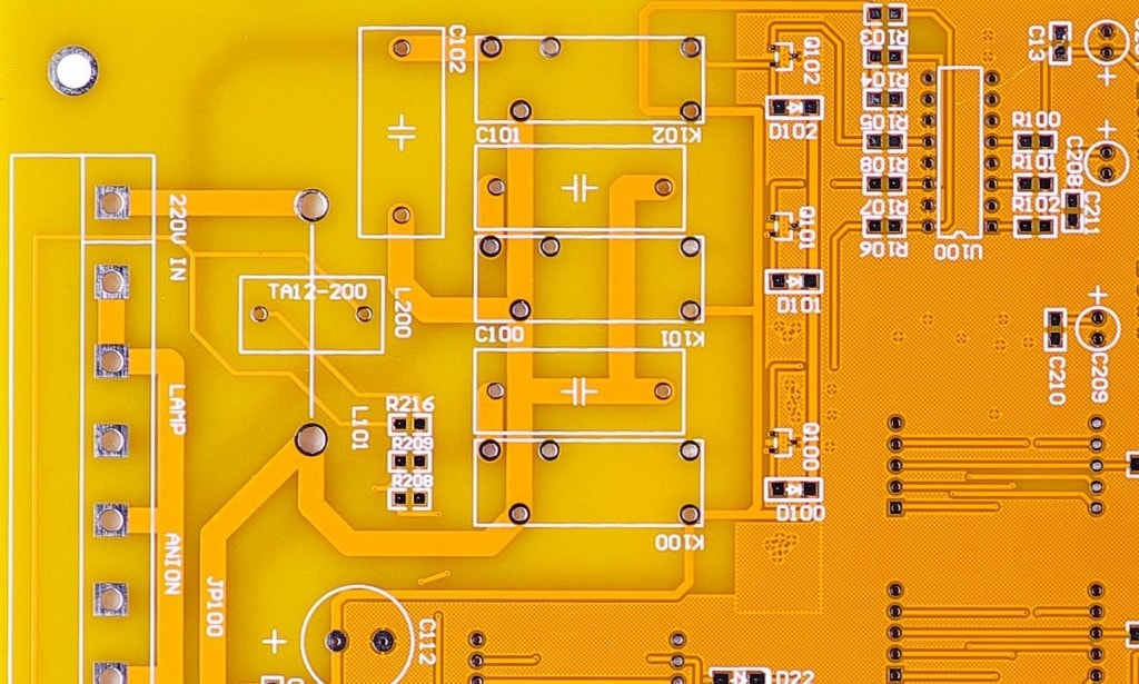
The surface finish of your printed circuit board might not be the first design aspect that you address in a new layout but it should be among the top contenders.
Where do you usually begin a PCB design? Mechanical design aspects would lead one to select rigid, flex, or bend-flex. Operating temperature would dictate if you required standard FR4, a high Tg version, a polyimide, PTFE, or ceramic. Microwave requirements might lead to a low dielectric constant and dissipation factor resin. Heat dissipation might require aluminum or copper core boards.
But what is required for the top surface where soldering and wire bonding takes place? The area where oxidation and metal migration occurs – have you addressed those concerns with a careful selection of surface finish?
The oldest PCB used finishes are 60Sn/40Pb solder (easily soldered at moderate temperatures but lead-containing) and OSP (very flat SMT pads but short shelf life). These were the mainstay of the industry so processing equipment, solder pastes, fluxes, solder masks, and even stencil inks were designed to handle those processing profiles.
The move to RoHS in Europe and later in the US (except for some mil spec and medical applications) resulted in development of lead-free SnAgCu solders based on tin with additions of silver and copper and with traces of bismuth, indium, zinc, and antimony. These pass the government RoHS regulations and after process development to minimize the growth of tin whiskers have become the mainstay of the industry. Initially the higher soldering liquidus temperature led engineers to specify high glass transition composite substrates (Tg 170-180°C) but careful attention to reflow profiles allowed a return to the less expensive standard Tg 135°C FR4 materials. Since the world industry has moved further toward RoHS many circuit board manufacturing plants have standardized on Pb-free HAL and no longer cost that surface at a premium. Indeed some have scrapped HASL entirely and subcontract that finish resulting in a cost premium for leaded solder.
 Another option, albeit more expensive than Pb-free HAL, is ENIG (electroless nickel/immersion gold). This surface, like OSP, renders the pads very flat and offers the additional advantage of longer shelf life and the ability to wire bond.
There is a low but measurable incidence of gold-to-nickel adhesion failure. This is called “black nickel” or “black pads” because, not surprisingly, the surface of the nickel turns black. The immersion gold on the pad surface looks normal and solder wets to the gold quite easily. However with any stress or even vibration the components could easily pop off without warning resulting from a brittle fracture at the interface. There are theories about phosphorous levels in the nickel plating solutions being off-spec and causing intermetallics during the gold plating. This problem is rare but does occur.
The most recent advance in surface preparation is ENEPIG, electroless nickel/electroless palladium/immersion gold. Typical thicknesses are 150-200 u” of nickel followed by 5 u” palladium and then 1-3 u” gold. There is a cost premium over ENIG but the advantages could far outweigh the price increase.
 In ENEPIG the palladium interlayer acts to protect the nickel layer during the gold plating process but dissolves into the solder during reflow, yielding an oxide-free activated site for an optimum bond to the components. The gold and palladium layers are inert and do not oxidize, resulting in excellent shelf life. Once the gold and palladium are dissolved during the soldering process the remaining layer of nickel prevents copper leaching into the solder.
For all of the advantages inherent in each surface treatment, what are the associated costs? The cost increase related to the precious metals is directly related to the surface area being plated, but given a typical mid-range circuit board a cost comparison would in today’s metals market yield:
|
Example PCB: 4-Layer 0.062” 1 oz FR4, 6.0” x 8.0”, various finishes |
||
|
Surface Treatment |
Cost per circuit board |
% increase vs HASL |
|
OSP |
$7.55 |
-1% |
|
HASL |
$7.55 |
0% |
|
Pb-free HAL |
$7.55 |
0% |
|
ENIG |
$8.60 |
14% |
|
ENEPIG |
$9.65 |
28% |
|
ENEPIG vs ENIG |
— |
12% |
The cost increase with ENEPIG compared to Pb-free HAL is significant but if it does the job, it is well worth the cost. On the other hand a 28% premium for ENEPIG or even the modest 14% increase with ENIG could be money wasted if your components do not demand the flattest of pads. Consider the processing parameters of your BoM early in the design process as their surface requirements will significantly affect the overall board cost.
If you have lingering doubts – call USTEK; we have the experience and know-how to answer your design questions! 614-538-8000 info@ustek.com

Comments are closed